IG Windows的問題,透過圖書和論文來找解法和答案更準確安心。 我們找到下列問答集和資訊懶人包
IG Windows的問題,我們搜遍了碩博士論文和台灣出版的書籍,推薦每日新聞採訪團隊寫的 失控的匿名正義:抹黑中傷、獵巫肉搜,你敲下的每個字都是傷人的利器 和楊比比的 我想學設計!人氣精選Photoshop影像編修技:工具x調色x文字x合成x廣告設計(千萬網友點擊推薦狂推必學)都 可以從中找到所需的評價。
另外網站How Can I Call On Instagram On PC? [Mac, Windows, Linux]也說明:There are a few ways to have an Instagram call on PC. You can use the web app, the mobile app, an emulator, or a developer tool.
這兩本書分別來自寶鼎 和碁峰所出版 。
長庚大學 電子工程學系 賴朝松所指導 Mamina Sahoo的 基於石墨烯及生物碳基材料的可撓式電晶體應用與能量攫取 (2021),提出IG Windows關鍵因素是什麼,來自於石墨烯、氟化石墨烯、太阳能电池、摩擦纳米发电机、生物碳、能量收集器。
而第二篇論文國立政治大學 傳播學院傳播碩士學位學程 林芝璇所指導 林伯育的 綠不綠由你-綠色化妝品廣告效果之探討 (2021),提出因為有 綠色化妝品、綠色廣告、消費者價值感知、廣告態度、購買意圖的重點而找出了 IG Windows的解答。
最後網站Instagram For PC: How To Post To Instagram Windows 10則補充:How to Download and Install Instagram Windows 10: · Open the Microsoft Store app · Search for the Instagram app · Click 'Get' and download · Once ...
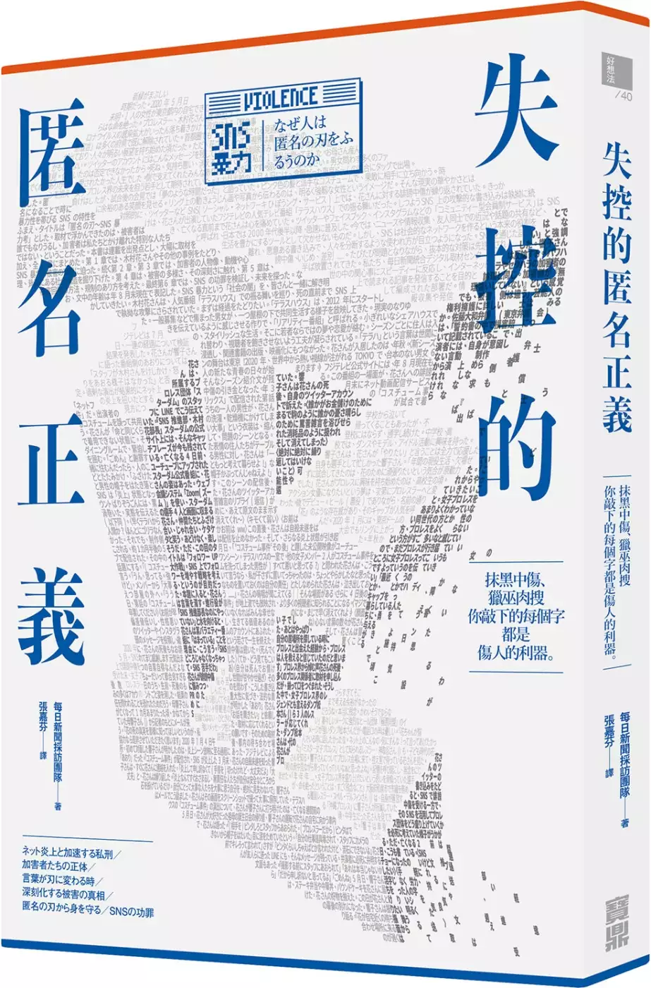
失控的匿名正義:抹黑中傷、獵巫肉搜,你敲下的每個字都是傷人的利器
為了解決IG Windows 的問題,作者每日新聞採訪團隊 這樣論述:
「木村花條款」通過! 混亂的失控正義迎來秩序 日本國會最新修法,網路霸凌者將被依法開罰! 「每天湧入近百則毫不留情地批評指教……去死、噁心、消失吧!一路走來,我比任何都還要強烈地這麼想。」 ——木村花/因《雙層公寓》「擂臺裝」事件被網友群起出征而走上絕路的職業摔角選手 「我發現要是被打,還會有『流血』這個看得到的實質損傷;但抹黑、中傷所帶來的『心傷』,是第三者看不到的。」——微笑菊池/因被影射為殺人兇手的不實謠言而遭受死亡威脅的日本諧星 「我覺得自己好像被三萬人監控,而且其中還有殺人魔王。」——土屋紫苑/因在推特發表對時事的感想評論而被網友攻擊的日本演員 「對我們這
些被害人而言,既看不到敵人的長相,也不知道石頭會從哪裡丟過來。這真的讓人痛苦至極,痛苦到心都被逼得走投無路。」——伊藤詩織/具名控訴遭上位者性侵,卻被網友嘲諷是「用身體換工作」的新聞工作者 「網友會把我沒說過的話塞到我嘴裡,還到處散播;或企圖惡意操作我的形象……」——石川優實/為女性歧視和政治議題發聲,因此飽受網友抨擊和性騷擾的演員兼模特兒 「豬頭、笨蛋、去死……雖然只是一些單純的謾罵,但一天出現好幾百則這種留言時,就會覺得全世界都這樣看我。」——春名風花/為自己支持的議題發聲而被網友惡意中傷的日本演員兼配音員 不只是公眾人物要遭受一句句惡評的無情傷害,就連一般素人也無法逃過
被私刑制裁: 2020年3月上旬,日本新冠肺炎疫情升溫時期,在節目上逆風發言的呼吸胸腔內科醫師,因言論被認為「反政府」導致上班的診所不斷接到電話騷擾;一名女性因確診後謊報足跡,她的本名、照片、工作地點、家人職業等都被肉搜出來,甚至有網站放出她公司的電話鼓舞網友打電話去告發…… 原本因匿名特性而充滿言論自由、包容多元聲音的社群媒體,為什麼會成為任何人都能肆意攻擊、難以咎責的灰色地帶?我們秉持的正義到底是誰的正義? 日本《每日新聞》團隊記者對現今網路霸凌亂象進行深入報導,讓讀者瞭解網路霸凌造成的危害與普病性。書中不僅探討當事者面臨霸凌及受到實際傷害時所承受的精神壓力和無助,也分析
網路這項匿名工具是如何加深群眾心理,讓許多如你我一般的平凡人在不知不覺之間化身為加害者。另外,本書也提出既有法律體制與環境對網路霸凌認知仍有所不足,條理性地分析應該如何改善。 ◎加害者就像路上隨處可見的普通人 因在現實生活中覺得不被理解,既孤單又缺乏罪惡感,網路成為確認自我、證明自己的場域。自己隨便打出的一句話能引來大量的贊同和回響,讓人感覺被網路上的社群所接納、包容。 ◎扭曲的正義,到頭來變成仇恨成癮 加害者發文攻擊的動機有兩種,一種是「看這話題炒得很熱我也要湊一腳」的「朝聖型」;一種是「我覺得你做錯了需要受點教訓」的「制裁型」。不論出於何種動機,被害人的反應例如出面反擊
或封鎖帳號,都會激化加害者行為,引起更激進的攻擊,像成癮一般。 ◎大眾媒體是網路公審火上添油的幫凶 調查發現,有近五成的民眾是從電視知道網路公審事件,而電視新聞報導的角度多半帶有譴責的偏頗性,導致民眾容易對遭受公審的對象有負面印象,並且透過新聞聳動的標題渲染,會吸引更多人參與,讓原本的網路公審事件再次延燒。 ◎社群媒體公司、政府都開始動作 推特訂定了一套「推特規則」,明文禁止用戶謾罵、脅迫或做出歧視行為,只要貼文被檢舉,就會執行刪除貼文或帳號停權等強制措施。各國政府也紛紛研擬應對的法條,像是加強管制仇恨言論的德國,就立法規定社群媒體公司需刪除涉及違法的貼文,否則將面臨天價罰
款。 ◎保障言論自由?先具備網路的使用素養吧 以法令限制效果有限,還會引發「言論自由已死」、「言論審查」的疑慮,根源的解方是提升是我們的網路使用素養,把網路上發生的事換成現實世界來思考,不會在現實世界做的事就不應該在網路上發生,並搞清楚批評指教與惡意中傷的界線。 當我們享受社群媒體匿名所帶來的便利性的同時,是否應負起相對應的責任?是否正確地使用這項工具?透過本書,一一審視社群媒體的功與過,並進一步探索未來可能落實的規範,避免悲劇再度重演! 本書特色 1.本書是由具公信力的媒體針對飽受矚目的社會議題進行剖析,敘事舉例條理分明,具可信度,例如備受矚目的「木村花」事件、遭受性
侵後勇敢出面發聲,反而承受更多網友「二度傷害」的伊藤詩織案例等。 2.本書不只是聚焦於發布惡意謾罵或威脅訊息的加害者,團隊更採訪諮商心理師、接觸過個案的律師等專業人士,深入剖析被害者無助的心理、一般人如何在無意之間造成特定人士傷害等諸多面向。 3.本書同時注重新的法律規範與「自由應建立於充分的公民素養之上」,期望透過務實手段改善社會的理想。 專業推薦 iWIN網路內容防護機構 王紹蓉/中山大學行銷傳播管理所所長 王雅涵/諮商心理師 朱家安/哲學雞蛋糕腦闆、作家 吳若權/作家、廣播主持、企管顧問 林靜如/律師娘 柯慧貞/臺灣網路成癮防治學會創會暨名譽理
事長 重點就在括號裡/影評人 海苔熊/心理學作家 許哲涵律師/律師真心話 蘇絢慧/諮商心理師 蘇益賢/諮商心理師 蘇予昕/蘇予昕心理諮商所所長、暢銷作家 (依姓氏筆劃排序)
IG Windows進入發燒排行的影片
大家好,你有在投資嗎?很多人說投資很難,
沒時間研究又怕有風險,其實只要有投資知識
對風險組合瞭解並找到自己適合的投資組合,
投資沒有那麼可怕,而且金額大小都可以!
不知道大家有沒有買過美股呢?
很多人都說不了解美股都離自己太遙遠了~
每天我們一早穿NIKE鞋玩instagram,
出門叫uber去上班,或使用windows電腦工作,
一個早上己經使用過將近十家美國上市公司的服務,
全球麼多人用的服務能不能賺錢可想而知!
很多人聽到美股就是擔心自己看不懂介面,
其實現在有更方便的交易平台可以使用~
SogoTrade這個平台己經成立了三十多年,
是一個多功能投資交易平台,
提供大家有簡繁中文的
投資美股、美股開戶、美股交易平台
股票,ETF,加密貨幣和期權,保證金交易及
動態投資組合。
美國國際帳戶無資本利得稅,換言之投資多少賺多少
產品種類齊全沒有額外費用,如帳戶維護費用,
管理費等,美股也無證所稅。
SogoTrade是合法的美國網絡證券公司,
提供網路美股投資平台,全中文介面,
免費中文美股資訊。
不受空間時間的限制,無論在哪個角落
都可以使用手機或電腦是最先進的網上交易平台,
可以方便又快速的進行交易
下單前要先做開戶,無須出國也可開設美股帳戶
網上線上開戶,待開通之後可使用,
SogoTrade 無交易佣金, 無帳戶維護費用 ,
還有每交易1000股贈送1美金獎勵
SogoTrade 也是合法加密貨幣交易平台,
像比特幣就是加密貨幣投資,
有些人不知道要去哪裡買,在這裡就可以!
線上開戶完成後,約七個工作天即可正式開通帳戶,
注資後即可交易。若有任何疑問請隨時致電,
SogoTrade 24小時中文客戶服務,
將隨時幫助您確認開戶進度與回答您的疑惑。
SogoTrade提供開戶會員免費美股中文資訊,
(點擊首頁的交易金點子) 早安美每日提供
中文版本的 8支個股分析,
對於不熟悉美股的投資人會是極大的幫助。
每天開盤前供大家八支短線熱點股票,
會包含目標價位等的重要訊息,
並且有圓形及指標體系滿足不同投資需求。
VALUENGINE 則提供免費詳細報告,
涵蓋選取市值股票兼顧高收益和低風險,
針對 SogoTrade 對會員提供的免費資訊作介紹,
可以幫助華語投資人更了解美股。
適用族群
股市新手
不會英文想投資美股的投資人
小資族
沒有美國國籍的投資人
不住在美國卻想投資美國股市的投資人
希望簡單交易的投資人
希望可以同時期權,ETF,股市,
加密貨幣甚至資產管的投資人
不想給台灣券商賺手續費者
想要進入國際股市朋友們。
靈活訂單輸入
互動式圖表
即時報價
盤前盤後交易
快速及高品質的訂單執行
全中文介面,無語言障礙
免費已翻譯中文的美股研究報告
24小時中文客服。
資美股、美股開戶、美股交易平台、
加密貨幣交易、期權交易都能輕鬆下單。
快速、簡單、功能強大且
有簡繁中文的美股交易在線平台,
集股票,ETF,加密貨幣和期權交易於一個網站。
不論您在世界哪個角落,皆可透過電腦或手機等
工具使用最先進的網上交易平台,
方便,快捷地進行交易。
跨國(非美國)線上開戶只要15分鐘,
24小時中文客服,打破語言與距離的障礙。
官網頁面:
https://tinyurl.com/yjlnk825
早安美股:
https://tinyurl.com/yjokpc7n
開通帳戶:
https://tinyurl.com/yzbqqmut
可投資產品頁面:
https://tinyurl.com/yg59aczs
-------------------------------------------------------------------------------------
妙妙琳己經出版著作有東京小日子一書
http://www.books.com.tw/products/0010794177
單曲幸福約定,KKBOX有上架
https://www.youtube.com/watch?v=NnbfrpQlQYU
當選群馬縣JR東日本觀光大使受邀參加六月份
非凡電視NEWS驚嘆號錄影,分享東京日本旅遊心得。
有在日本生活一年多的遊學經驗。
歡迎和妙妙琳一起看美好世界
痞客幫
http://miumiuloveu.pixnet.net/blog
STYLE ME美妝時尚人物專欄
https://styleme.pixnet.net/authors/miumiuloveu
粉絲專頁-Miu Miu Lin妙妙琳日本就學工作奮鬥記
https://www.facebook.com/miumiuloveu
IG
https://www.instagram.com/miumiulin221/
基於石墨烯及生物碳基材料的可撓式電晶體應用與能量攫取
為了解決IG Windows 的問題,作者Mamina Sahoo 這樣論述:
Table of ContentsAbstract.......................................................................................................iFigure Captions........................................................................................xiTable Captions...................................................
....................................xxiChapter 1: Introduction1.1 Flexible electronics................................................................................11.2 Graphene the magical material ………………………….……….......21.2.1 Synthesis of graphene…………………………….….…...21.2.1.1 Mechanical exfoliati
on of graphene………………...……21.2.1.2 Epitaxial growth on Sic substrate………………….…..31.2.1.3 Chemical vapor deposition (CVD) method………….…..41.2.2 Graphene transfer…………………………………………....41.3 Application of graphene based Electronics……………………….......51.3.1 Graphene based flexible transparent electrode
……………….61.3.2 Top gated Graphene field effect transistor…………………….71.4 Challenges of flexible graphene based field effect transistors.……….91.5 Energy harvesting devices for flexible electronics………….........….91.6 Solar cell…………………………………………………………...101.6.1 Device architecture…………………………………………101.
6.2 Issues and Challenges of Perovskite solar cells………...121.7 Triboelectric nanogenerator (TENG)………………………………121.7.1 Working mode of TENG………………………………….141.8 Applications of TENG………………………………………………151.8.1 Applications of graphene based TENG…………………....151.8.2 Applications of bio-waste material ba
sed TENG………….171.9 Key challenges of triboelectric nanogenerator…………………....…191.10 Objective and scope of this study………………………………....19Chapter 2: Flexible graphene field effect transistor with fluorinated graphene as gate dielectric2.1 Introduction………………………………………………………....212.2 Material preparation a
nd Device fabrication………………. 232.2.1CVD Growth of Graphene on Copper Foil………………….232.2.2 Transfer of graphene over PET substrate……………...........252.2.3 Fabrication of fluorinated graphene ……………...........252.2.4 F-GFETs with FG as gate dielectric device fabrication……262.2.5 Material and electrical C
haracterization …………………272.3 Results and discussion…………………………………………….282.3.1 Material characterization of PG and FG……………...…...….282.3.2 Electrical characterization of F-GFET with FG as dielectrics..332.3.3 Mechanical stability test of F-GFET with FG as dielectrics ….362.4 Summary…………………………………………………
………....40Chapter 3: Robust sandwiched fluorinated graphene for highly reliable flexible electronics3.1 Introduction………………………………………………………….423.2 Material preparation and Device fabrication ………………….........443.2.1 CVD Growth of Graphene on Copper Foil…………………...443.2.2 Graphene fluorination …...…….…………
…………..............443.2.3 F-GFETs with sandwiched FG device fabrication....................443.2.4 Material and electrical Characterization…..............................453.3 Results and discussion ……………………………………...............453.3.1 Material characterization of sandwiched…………………….453.3.2 Electric
al characterization of F-GFET with sandwiched FG....473.3.3 Mechanical stability test of F-GFET with sandwiched FG…503.3.4 Strain transfer mechanism of sandwiched FG………………513.4 Summary…………………………………………………………....53Chapter 4: Functionalized fluorinated graphene as a novel hole transporting layer for ef
ficient inverted perovskite solar cells4.1 Introduction………………………………………………………….544.2 Material preparation and Device fabrication......................................564.2.1 Materials ………………………...…………………………564.2.2 CVD-Graphene growth ……………………………...…...564.2.3 Graphene fluorination …………………………………….564.
2.4 Transfer of fluorinated graphene…………………………...574.2.5 Device fabrication …………………………………….….574.2.6 Material and electrical Characterization …….....................584.3 Results and discussion …………………………………………….594.3.1 Surface electronic and optical properties of FGr……….….594.3.2 Characterization o
f FGr and perovskite surface ……….…644.3.3 Electrical performance of PSC………………….…….…...694.3.4 Electrical performance of Flexible PSC……………………724.4 Summary…………………………………………………………...78Chapter 5: Flexible layered-graphene charge modulation for highly stable triboelectric nanogenerator5.1 Introduction…………
…………………………………………....795.2 Experimental Section……………………………………………….825.2.1 Large-area graphene growth ……………………………….825.2.2 Fabrication of Al2O3 as the CTL …………………………...825.2.3 Fabrication of a Gr-TENG with Al2O3 as the CTL………825.2.4 Material characterization and electrical measurements…….835.3 Results
and discussion.…………………………………...…………845.3.1 Material Characterization of Graphene Layers/Al2O3……845.3.2 Working Mechanism of Gr-TENG with Al2O3 as CTL…915.3.3 Electrical Characterization of Gr-TENG with Al2O3 CTL…945.3.4 Applications of the Gr-TENG with Al2O3 as CTL……….1015.4 Summary…………………………………………
……………….103Chapter 6: Eco-friendly Spent coffee ground bio-TENG for high performance flexible energy harvester6.1 Introduction…………………………………………………….......1046.2 Experimental Section…………………………………………….1086.2.1 Material Preparation …………………………………….1086.2.2 Fabrication of SCG powder based TENG………………...1086
.2.3 Fabrication of SCG thin-film based TENG ………………1096.2.4 Material characterization and electrical measurements….1106.3 Results and discussion.…………………………………...………1116.3.1 Material Characterization of SCG powder and thin film….1116.3.2 Working Mechanism of SCG-TENG……………………...1186.3.3 Electrical Cha
racterization of SCG-TENG……………….1226.3.4 Applications of the SCG thin-film based TENG………….1326.4 Summary………………………………………………………….134Chapter 7: Conclusions and future perspectives7.1 Conclusion………………………………………………………....1357.2 Future work …………………………….………………………….1377.2.1 Overview of flexible fluorinated g
raphene TENG..............1377.2.1.1 Initial results………………………………….…1387.2.2.1.1 Fabrication of FG-TENG………………1387.2.2.1.2 Working principle of FG-TENG……….1397.2.2.1.3 Electrical output of FG-TENG.………...140References…………………………………………………………….142Appendix A: List of publications………………….……………..........177A
ppendix B: Fabrication process of GFETs with fluorinated graphene (FG) as gate dielectric……........……………………………………….179Appendix C: Fabrication process of GFETs with sandwiched FG…....180Appendix D: Fabrication process of inverted perovskite solar cell with FGr as HTL…………………………………………………………….181Appendi
x E: Fabrication of a Gr-TENG with Al2O3 as the CTL…….182Appendix F: Fabrication of SCG based triboelectric nanogenerator….183Figure captionsFigure 1-1 Exfoliated graphene on SiO2/Si wafer……………………….3Figure 1-2 Epitaxial graphene growth on SiC substrate………………....3Figure 1-3 Growth mechanism of graphe
ne on Cu foil by CVD ……......4Figure 1-4 Wet transfer process of CVD grown graphene…………...….5Figure 1-5 RGO/PET based electrodes as a flexible touch screen.……....6Figure 1-6 Graphene based (a) touch panel (b) touch-screen phone…….7Figure 1-7 Flexible graphene transistors (a) (Top) Optical photograph
of an array of flexible, self-aligned GFETs on PET. (Bottom) The corresponding schematic shows a device layout. (b) Schematic cross-sectional and top views of top-gated graphene flake–based gigahertz transistors. (Left) AFM image of a graphene flake. (Right) Photograph of flexible graphene devices
fabricated on a PI substrate. (c) Cross-sectional schematic of flexible GFETs fabricated using a self-aligned process……8Figure 1-8 The magnitude of power needed for meet certain operation depending critically on the scale and applications………………………10Figure 1-9 Schematic diagrams of PSC in the (a) n-i
-p mesoscopic, (b) n-i-p planar, (c) p-i-n planar, and (d) p-i-n mesoscopic structures………...12Figure 1-10 Schematic illustration of the first TENG...………………...13Figure 1-11 Working modes of the TENG. (a) The vertical contact-separation mode. (b) The lateral sliding mode. (c) The single-electrode mode
. (d) The free-standing mode ………………………………...……14Figure 1-12 Schematic illustration of (a) device fabrication of graphene-based TENGs (b) graphene/EVA/PET-based triboelectric nanogenerators (c) device fabrication of stretchable CG based TENG with electrical output performance……………………………………………………...17
Figure 1-13 Schematic illustration and output performance of bio-waste material based TENG (a) Rice-husk (b) Tea leaves (c) Sun flower powder (SFP) (d) Wheat stalk based TENG………….…………………………18Figure 2-1 Graphene synthesis by LPCVD method……….…………...24Figure 2-2 Schematic diagram of (a) preparation pro
cess of 1L-FG/copper foil (b) Layer by layer assembly method was used for fabricating three-layer graphene over copper foil and then CF4 plasma treatment from top side to form 3L-FG/copper foil…………………….26Figure 2-3 Schematic illustration of fabrication process of F-GFET with FG as gate dielectric ……
……………………………………………….27Figure 2-4 (a) Raman spectra of PG, 1L-FG and 3L-FG after 30 min of CF4 plasma treatment over copper foil. (b) Peak intensities ratio ID/IG and optical transmittance of PG, 1L-FG and 3L-FG. Inset: image of PG and 1L-FG film over PET substrate. (c) Typical Raman spectra of PG, 1L
-FG and 3L-FG on PET substrate. (d) Optical transmittance of PG, 1L-FG and 3L-FG film over PET substrate. The inset shows the optical image of GFETs with FG as gate dielectrics on PET ……….…………30Figure 2-5 XPS analysis result of (a) PG (b) 1L-FG (c) 3L-FG where the C1s core level and several carbon f
luorine components are labeled. The inset shows the fluorine peak (F 1s) at 688.5 eV……………………….32Figure 2-6 (a) Water contact angle of PG, 1L-FG and 3L-FG over PET substrate. (b) The relationship between water contact angle of PG, 1L-FG and 3L-FG and surface-roughness………………………………………33Figure 2-7 (a) I
d vs. Vd of w/o-FG, w/1L-FG and w/3L-FG samples after 30 min of CF4 plasma (b) Id vs. Vg of w/o-FG, w/1L-FG and w/3L-FG samples at a fixed value of drain to source voltage, Vds of 0.5 V (c) Gate capacitance of w/o-FG, w/1L-FG and w/3L-FG samples (d) Gate leakage current of w/o-FG (naturally formed A
l2OX as gate dielectric), w/1L-FG and w/3L-FG samples ……………………………...…………...……...34Figure 2-8 (a) Schematic illustration of bending measurement setup at different bending radius. (i) Device measurement at (i) flat condition (ii) bending radius of 10 mm (iii) 8 mm (iv) 6 mm. Inset shows the photograph
of measurement setup. Change in (b) carrier mobility (c) ION of w/o-FG, w/1L-FG and w/3L-FG samples as a function of bending radius. The symbol ∞ represents the flat condition. Change in (d) carrier mobility (e) ION of w/o-FG, w/1L-FG and w/3L-FG samples as a function of bending cycles (Strain = 1.
56%)…………………………………….38Figure 3-1 Schematic illustration of the flexible top gate graphene field effect transistor with sandwich fluorinated graphene (FG as gate dielectric and substrate passivation layer) ……………………………...…………44Figure 3-2 Raman spectra of (a) PG/PET and PG/FG/PET substrate (b) sandwiche
d FG (FG/PG/FG/PET). Inset showing the optical transmittance of sandwiched FG. (c) HRTEM image for 1L-FG.……………….….…46Figure 3-3 (a) Id vs. Vd of FG/PG/FG device at variable vg (−2 to 2 V). (b) Id vs. Vg of FG/PG/FG. (c) Gate capacitance of FG/PG/FG ….…….48Figure 3-4 Raman spectra of devices under be
nding (a) PG/PET (Inset shows the 2D peak) (b) PG/FG/PET (inset shows the 2D peak) …….…49Figure 3-5 (a) Change in Mobility (b) change in ION of PG/PET and PG/FG/PET as a function of bending radius between bending radii of ∞ to 1.6 mm in tensile mode (c) Change in Mobility (d) Change in ION of PG/PET
and PG/FG/PET as a function of bending cycles. Inset of (c) shows the photograph of F-GFETs with sandwich FG on the PET substrate (e) change in resistance of w/1L-FG, 1L-FG/PG/1L-FG samples as a function of bending radius ………………………...……………….50Figure 3-6 Schematic evolution of proposed strain transf
er mechanism through PG/PET and PG/FG/PET. The inset of PG/PET sample shows the generation of sliding charge due to interfacial sliding between PG and PET ………………………………………………………………….….52Figure 4-1 FGr fabrication and transfer process …………….………....57Figure 4-2 (a) Raman analysis of pristine graphene a
nd the FGr samples after 5, 10, 20, and 30 min of CF4 plasma treatment over Cu foil (b) Raman intensity ratios (I2D/IG and ID/IG) of fluorinated graphene, with respect to the exposure time ……………………………………………60Figure 4-3 SEM images of (a) ITO, (b) ITO/1L-FGr, (c) ITO/2L-FGr, and (d) ITO/3L-FGr …………………
………………………………….61Figure 4-4 XPS analysis of FGr with (a) 5 min (b) 10 min and (c) 20 min of CF4 plasma treatment on the Cu foil (d) The fluorine peak (F1s) of FGr (f) The correlation of the carbon-to-fluorine fraction (C/F) with exposure time and the corresponding carrier concentrations …………….………62Fi
gure 4-5 Tauc plots and UV–Vis absorption spectra of FGr films with CF4 plasma treatment for (a) 5, (b) 10, and (c) 20 min ….………......….63Figure 4-6 WCAs on PEDOT: PSS and 1L, 2L, and 3L FGr samples ...64Figure 4-7 (a) Mechanism of large grain growth of perovskite on a non-wetting surface (b) Top-vi
ew and cross-sectional surface morphologies of perovskites on various HTLs ………………………………...…………65Figure 4-8 XRD of perovskite films on various HTL substrates ….…...66Figure 4-9 UPS spectra of various numbers of FGr layers on ITO: (a) cut-off and (b) valance band spectra …………………………………….….67Figure 4-10
Energy band diagrams of PSCs with (a) PEDOT: PSS, (b) 1L-FGr, (c) 2L-FGr, and (d) 3L-FGr as HTL …………………….…….68Figure 4-11 (a) Steady state PL spectra of PEDOT: PSS/perovskite and FGr/perovskite films. (b) TRPL spectral decay of PEDOT: PSS/perovskite and FGr/perovskite films………………………….……69Figure 4-1
2 (a) Schematic representation of a PSC having an inverted device configuration. (b) Cross-sectional HRTEM image of the ITO/ FGr–perovskite interface………………………………………...………70Figure 4-13 Photovoltaic parameters of PSCs incorporating various HTL substrates: (a) PCE (%), (b) Voc (V), (c) Jsc (mA/cm2), an
d (d) FF (%)....71Figure 4-14 Normalized PCEs of target and control PSCs incorporating various HTL substrates, measured in a N2-filled glove box. (a) Thermal stability at 60 °C (b) Light soaking effect under 1 Sun (c) Stability after several days …………………………………………………………….72Figure 4-15 (a) Schematic r
epresentation of the structure of a flexible PSC on a PET substrate (b) J–V curves of control and target flexible PSCs, measured under both forward and reverse biases. (c) Average PCE of flexible PSCs incorporating PEDOT: PSS and FGr HTLs……….…73Figure 4-16 (a) Normalized averaged PCEs of the flexibl
e PSCs after bending for 10 cycles at various bending radii. (b) Normalized averaged PCEs of the flexible PSCs plotted with respect to the number of bending cycles at a radius of 6 mm ………………………………………………75Figure 4-17 Photovoltaics parameters of flexible PSCs with various HTL substrates: (a) JSC (mA/c
m2), (b) Voc (V), and (c) FF (%) ……………....75Figure 4-18 XRD patterns of perovskite films on PET/ITO/FGr, recorded before and after bending 500 times …………………………………….76Figure 4-19 SEM images of (a) perovskite films/FGr/ITO/PET before bending (b) after bending 500 times (c) perovskite films/PEDOT: PSS/
ITO/PET before bending (d) after bending 500 times ……………….…77Figure 4-20 PL spectra of perovskite films on PET/ITO/FGr, recorded before and after various bending cycles …………………………….…78Figure 5-1 Schematic illustration showing the fabrication process of a flexible Gr-TENG with Al2O3 as the CTL ……………
………………...83Figure 5-2 The Raman spectra of (a) graphene/Al-foil/PET and (b) graphene/Al2O3/Al-foil/PET. The I2D/IG of graphene layers (1L, 3L and 5L) over (c) Al-foil/PET substrate (d) Al2O3/Al-foil/PET substrate …...85Figure 5-3 XRD patterns of (a) graphene/Al-foil/PET and (b) graphene/Al2O3/Al-foi
l/PET ……………………………………………86Figure 5-4 FESEM image of the graphene surface on (a) Al-foil/PET and (b) Al2O3/Al-foil/PET. EDS analysis of (c) graphene/Al-foil/PET and (d) graphene/Al2O3/Al-foil/PET (e) EDS elemental mapping of the graphene/Al2O3/Al-foil/PET presenting C K series, O K series and Al K ser
ies …………………………………………………………….………87Figure 5-5 3D AFM images of (a) 1L-Gr (b) 3L-Gr (c) 5L-Gr on Al foil (d) 1L-Gr (e) 3L-Gr (f) 5L-Gr on Al2O3/Al foil………………….….….89Figure 5-6 Work function of graphene layers on the (a) Al-foil (b) Al2O3/Al-foil substrate by KPFM. Inset showing the surface potential of
graphene layers (1L, 3L and 5L) over Al-foil and Al2O3 substrate (c) energy band diagrams for 1L-Gr, 3L-Gr and 5L-Gr over Al2O3 ……....90Figure 5-7 Schematic illustration of Electronic energy levels of graphene samples and AFM tip without and with electrical contact for three cases: (i) tip and the
1L-Gr (ii) tip and the 3L-Gr and (iii) tip and the 5L-Gr over Al2O3/Al foil/PET……………………………………….…...…………91Figure 5-8 Working mechanism of Gr-TENG with Al2O3 ….….…...…93Figure 5-9 a) ISC and (b) VOC of 1L-, 3L- and 5L-Gr-TENGs without Al2O3 CTL (c) Sheet resistance of graphene as a function of number
of layers ………………………………...…...…………………………….95Figure 5-10 Electrical output of the Gr-TENG with Al2O3 CTL: (a) ISC and (b) VOC of 1L-, 3L- and 5L-Gr. Magnification of the (c) ISC and (d) VOC of the 3L-Gr-TENG with Al2O3 as the CTL. Average mean (e) ISC and (f) VOC generated by pristine Gr-TENGs (1L, 3L
and 5L) and Gr-TENGs (1L, 3L and 5L) with Al2O3 CTL. Error bars indicate standard deviations for 4 sets of data points ……………...…………….….…......96Figure 5-11 (a) CV of Al/Al2O3/3L-Gr/Al at 100 kHz and 1 MHz (b) CV hysteresis of 3L-Gr-TENG with Al2O3 as CTL with different sweeping voltages (c) Surface
charge density of graphene (1L, 3L and 5L)-based TENG with and without Al2O3 as CTL ………………………………...98Figure 5-12 Circuit diagram of output (a) VOC and (b) ISC measurement of 3L-Gr TENG with Al2O3 CTL as a function of different resistors as external loads. Variation in VOC and ISC w.r.t different re
sistors as external loads of (c) 3L-Gr TENG with Al2O3 CTL (d) 3L-Gr TENG without Al2O3 CTL. Relationship between electrical output power and external loading resistance (e) 3L-Gr TENG with Al2O3 CTL (f) 3L-Gr TENG without Al2O3 CTL…………………………………….………………...99Figure 5-13 (a)Electrical stability and du
rability of the 3L-Gr TENG with Al2O3 (b) Schematic illustrations showing the charge-trapping mechanism of 3L-Gr-TENG without and with Al2O3 charge trapping layer ………101Figure 5-14 (a) Photograph showing 20 LEDs being powered (b) Circuit diagram of bridge rectifier (c) Charging curves of capacitors
with various capacitances (d) Photograph of powering a timer …….………………102Figure 6-1 The schematic diagram of the fabrication process for SCG powder based TENG ……………………………………………….….108Figure 6-2 The schematic diagram of the fabrication process for SCG thin-film based TENG via thermal evaporation meth
od ………………109Figure 6-3 FESEM image of (a) SCG powder (inset image illustrates the high magnification of SCG powder) (b) SCG thin-film/Al foil/PET (inset image illustrates the high magnification of SCG thin-film). EDS of the (c) SCG powder (d) SCG thin-film/Al foil/PET…………………………. 112Figure 6-4 Raman
spectra analysis (a) pristine SCG powder (b) SCG thin-film/Al foil/PET. XRD patterns of (c) SCG powder (d) SCG thin film with different thickness ……………………………………… ……….115Figure 6-5 FTIR analysis of the (a) pristine SCG powder sample (b) SCG thin film………………………………………………………………...116Figure 6-6 3D AFM ima
ge of SCG thin-film with various thickness (a) 50 nm (b)100 nm and (c) 200 nm……………………………………...117Figure 6-7 Schematic illustration of working principle of SCG thin-film based TENG …………………………………………………………...119Figure 6-8 Finite element simulation of the generated voltage difference for SCG thin-film b
ased TENG based on the contact and separation between SCG thin film and PTFE …………….……………………….120Figure 6-9 (a) The setup for electrical property testing, which including a Keithley 6514 system electrometer and linear motor. Electrical output (b) ISC (c) VOC of TENGs based on different friction pairs
for checking the triboelectric polarity of SCG…………………………………………...123Figure 6-10 Electrical measurement of (a) ISC and (b) VOC of the SCG thin-film based TENG. Mean value of (d) ISC (e) VOC and (f) Output power density of the pristine SCG powder and thermal deposited SCG thin-film based TENG. ...………
………………………………………125Figure 6-11 (a) Schematic illustration of KPFM for measuring the work function. (b) Surface potential images of SCG thin film with various thickness (50 nm, 100 nm and 200 nm). (c) Surface potential and (d) Work function vs SCG thin film with various thickness (50 nm, 100 nm and 20
0 nm).………….……………………………………………….128Figure 6-12 (a) Isc and (b) Voc of SCG thin film based TENG under different contact frequencies (c) Isc and (d) Voc of SCG thin film based TENG under different separation distance…………………………….129Figure 6-13 Electrical response (a) ISC (b) VOC of pristine SCG powder an
d (c) ISC (d) VOC of SCG thin-film based TENG with respect to different relative humidity (35-85% RH) …………………………….131Figure 6-14 Electrical stability and durability test of the output performance of (a) pristine SCG powder based TENG (b) SCG thin-film based TENG……………………………………………………………132Figure 6-15
Applications of the SCG thin film based TENG as a power supply: (a) Circuit diagram of the bridge-rectifier for charging a capacitor (b) Charging curves of capacitors with various capacitances (0.1, 2.2 and 3.3 µF) (c) Photograph of powering a timer…………………...………133Figure 7-1 Schematic illustration o
f FG based TENG…….….……….139Figure 7-2 Working mechanism of FG based TENG…………………140Figure 7-3 Electrical output of FG-TENG: (a) Isc and (b) Voc …….….141Table captionsTable 2-1 Comparison of flexible G-FETs on/off ratio of our work with other’s work…………………………………………………...………...40Table 3-1 Summary of th
e electrical and mechanical performance of flexible w/o-FG, w/ 1L-FG, w/3L-FG and sandwich FG (FG/PG/FG) samples......................................................................................................52Table 3.2: Comparison of the electrical and mechanical performance of sandwich FG ba
sed F-GFET with previous F-GFET with different gate dielectrics……………………………………………………….………53Table 4-1 Best photovoltaic performance from control and target devices prepared on rigid and flexible substrates……………………………......74Table 5-1 EDS elemental analysis of graphene over Al-foil/PET and Al2O3/Al-foi
l/PET ………………………………………………………88Table 5-2 Comparison of electrical output performance of Gr-TENGs with and without Al2O3 CTL samples used in this study………………103Table 6-1 EDS elemental analysis of SCG-Powder and SCG thin film /Al foil/PET………………………………………………………………...113Table 6-2 Comparison of electrical o
utput performance of SCG-TENGs samples used in this study……………………………………………...126
我想學設計!人氣精選Photoshop影像編修技:工具x調色x文字x合成x廣告設計(千萬網友點擊推薦狂推必學)

為了解決IG Windows 的問題,作者楊比比 這樣論述:
看書學Photoshop不容易 除了強大的自律性、超人的毅力 還需要技巧補充 與 無所不在的叮嚀 --- 我是陪著大家一起努力的楊比比 你也想學設計嗎?但總覺得很難不知從何著手? 「PS 了嗎?」,Photoshop已儼然成為影像編修的代名詞,學設計當然就要從業界最多人使用的Photoshop入門! 楊比比由多年教學經驗精選出大家最想學的Photoshop編修技巧,包括IG熱門色調、補色拼貼、數位濾鏡、行動裝置用檔案、脫穎而出的文字排版、文字外框變形技巧、快速去背、逼真合成…,其獨特且輕鬆幽默的教學方式讓你看的清楚、學的容易。 75個獨家技巧不藏私大公開 每個範例
都是楊比比整理出影像編修最有效率的步驟,帶你呈現出更自然的影像合成與色調: —懷舊氣氛十足還有細膩的色調變化 —明暗之間強化照片立體感與層次 —全自動色調修復泛黃照片絕佳的工具 —極受歡迎的半網屏風格 —設定適合行動裝置使用的工作區 —相近色容易配出好看的漸層色彩 —快又精準的數位換色 —折角立體堆疊文字效果 —建立只有外框線的羅馬垂直字 —移除圖片中多餘範圍 —精細去背技法移除雜色、毛髮去背 —運用顏色建立選取範圍 —商業用路徑去背 —數位時代新設計的扁平化Logo —逼真的岩石雕像合成技法 快翻開書看更多精彩技巧吧! 本
書以有系統的教學方式搭配楊比比二十幾年的教學經驗及獨特的美感,帶你領略影像編修的魅力。 如果你是設計初學者,別怕!跟著內容操作就能完成意想不到的作品! 如果你已是設計老手,本書範例將讓你對設計有不同的體會,激發出更多靈感! 想自學Photoshop?本書提供精彩範例檔,只要跟著書本操作,一定學的會! 想當授課用書?完整全面的內容規劃搭配多樣化的範例,與業界實戰無縫接軌!
綠不綠由你-綠色化妝品廣告效果之探討
為了解決IG Windows 的問題,作者林伯育 這樣論述:
氣候變遷與環境汙染等災難促使人們不得不重視環境永續的議題。其中,化妝品產業為了因應全球永續發展的目標,積極開發天然與有機的綠色化妝品市場,希望以綠色屬性的產品吸引環保潮流中,越發關注環境保護的消費者。但產業發展至今,消費者對於綠色化妝品的具體定義,似乎仍存在模糊空間,此外,雖然環境保護的綠色趨勢正逐年上升,但對比不具綠色屬性的一般化妝品,綠色化妝品真的有比較吸引消費者嗎?本研究將廣告訴求與產品類別做為自變項,設計雙因子實驗(廣告訴求:環境永續訴求/價格促銷訴求,產品類別:綠色化妝品/一般化妝品),並將消費者價值感知、廣告態度作為中介變項,購買意圖為依變項。研究採線上實驗法,以Instagra
m限時動態為刺激物操弄的媒介,並獲得243份有效樣本。研究結果顯示,環境永續訴求的化妝品廣告在消費者價值感知與購買意圖都顯著高於價格促銷訴求;廣告訴求跟產品類別僅在少數情況下具有交互作用:當廣告運用環境永續訴求時,兩種產品對消費者價值感知面向皆無顯著差異;當廣告運用價格促銷訴求時,綠色化妝品訊息對情感價值感知及條件價值感知的影響顯著高於一般化妝品。然而,僅有部分消費者價值感知(功能價值感知、社會價值感知、新奇價值感知)會正向影響廣告態度,而廣告態度會正向影響購買意圖。此外,檢驗連續中介模型後發現,在價格促銷訴求下,綠色化妝品比一般化妝品更能正向影響社會價值感知,並接續正向影響廣告態度,進而提升
購買意圖。本研究進一步探討研究結果的學術與實務意涵,並提出研究限制與建議,供未來相關研究參考。